LiFePO4wered/Solar4 prototype PCB assembly
Assembly
I received the prototype PCBs from JLCPCB so it was time to assemble and test them. As usual, I had ordered a stencil so it was a straightforward process of applying solder paste, hand populating components and reflow.
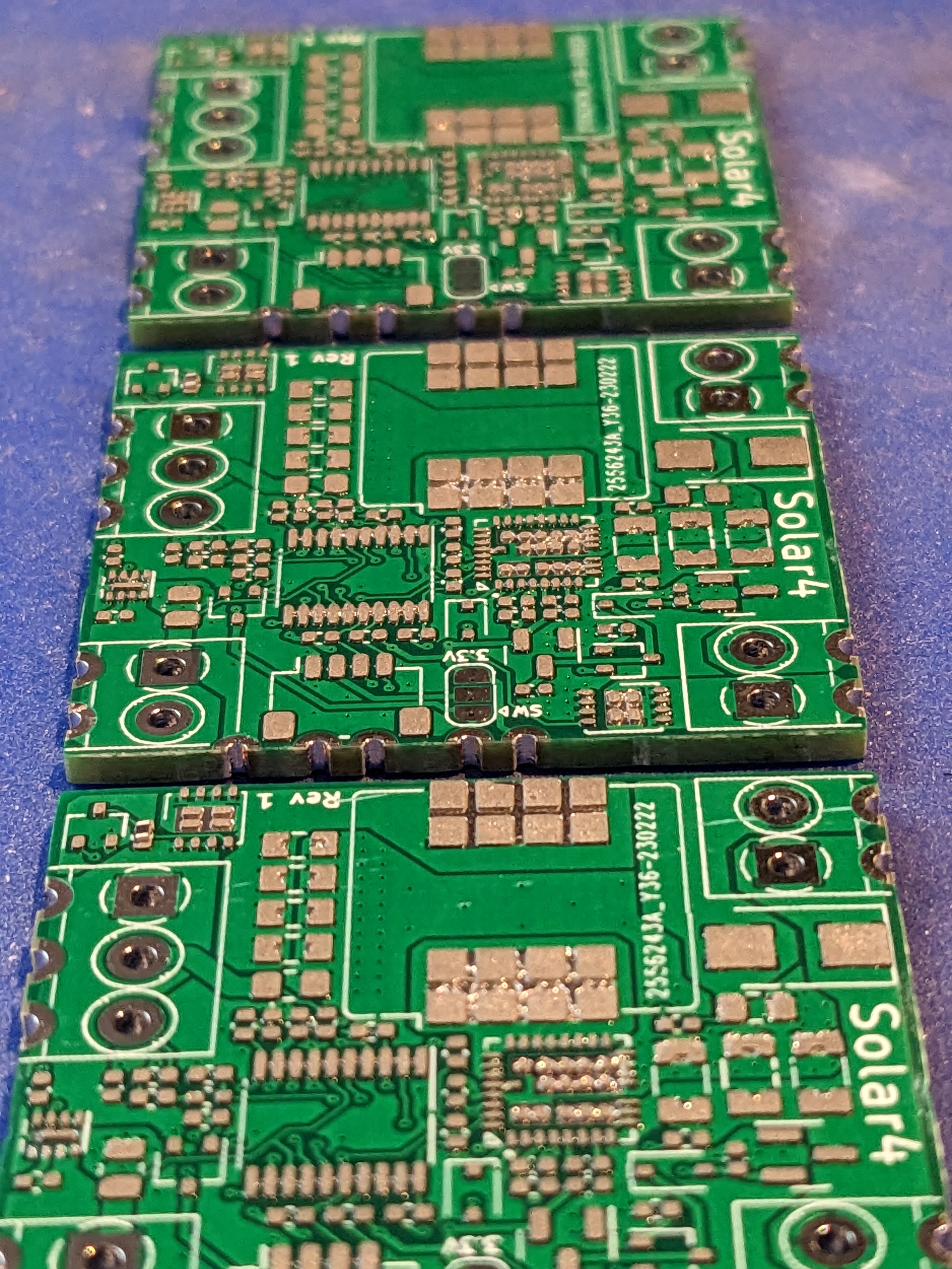
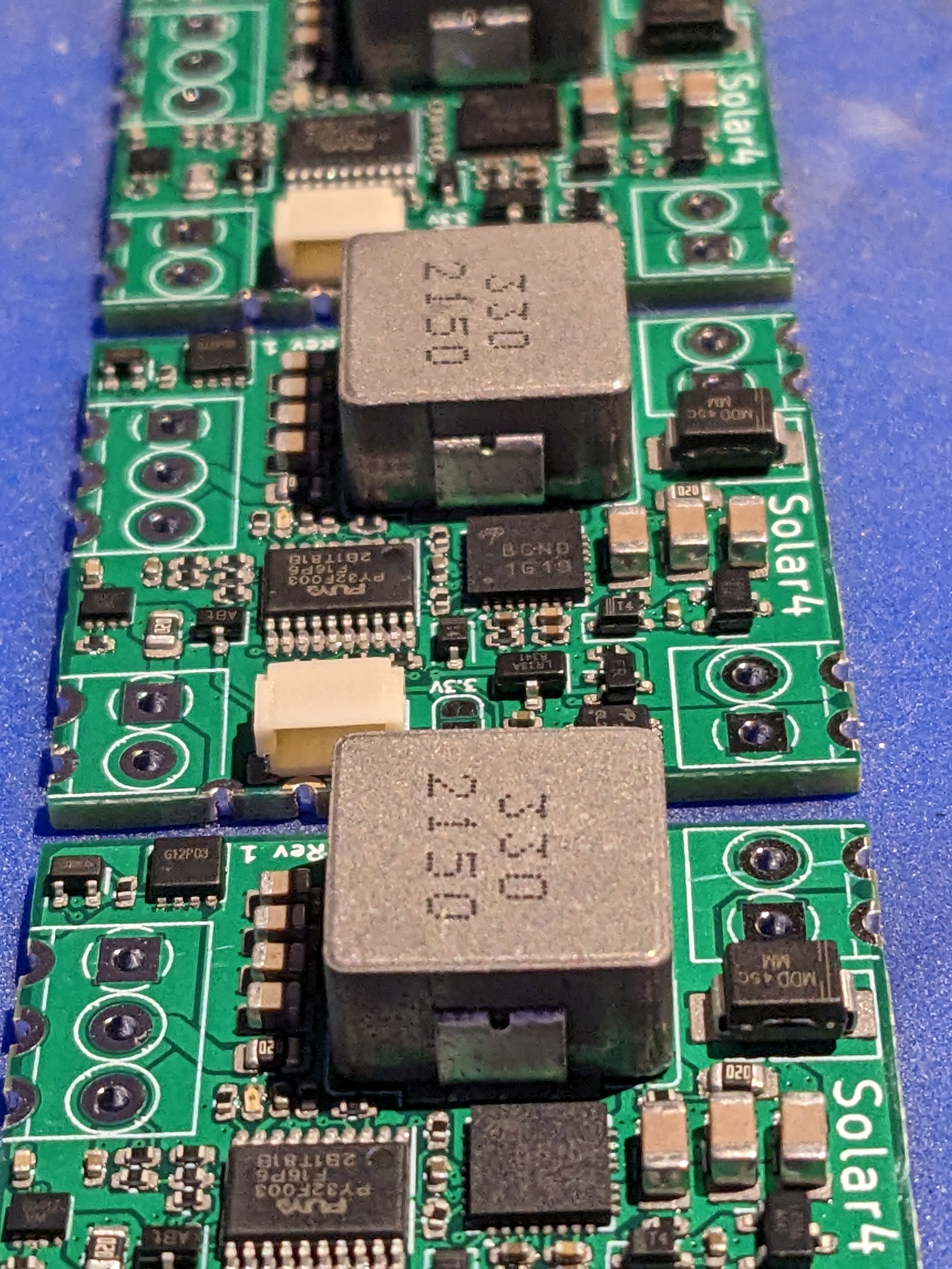
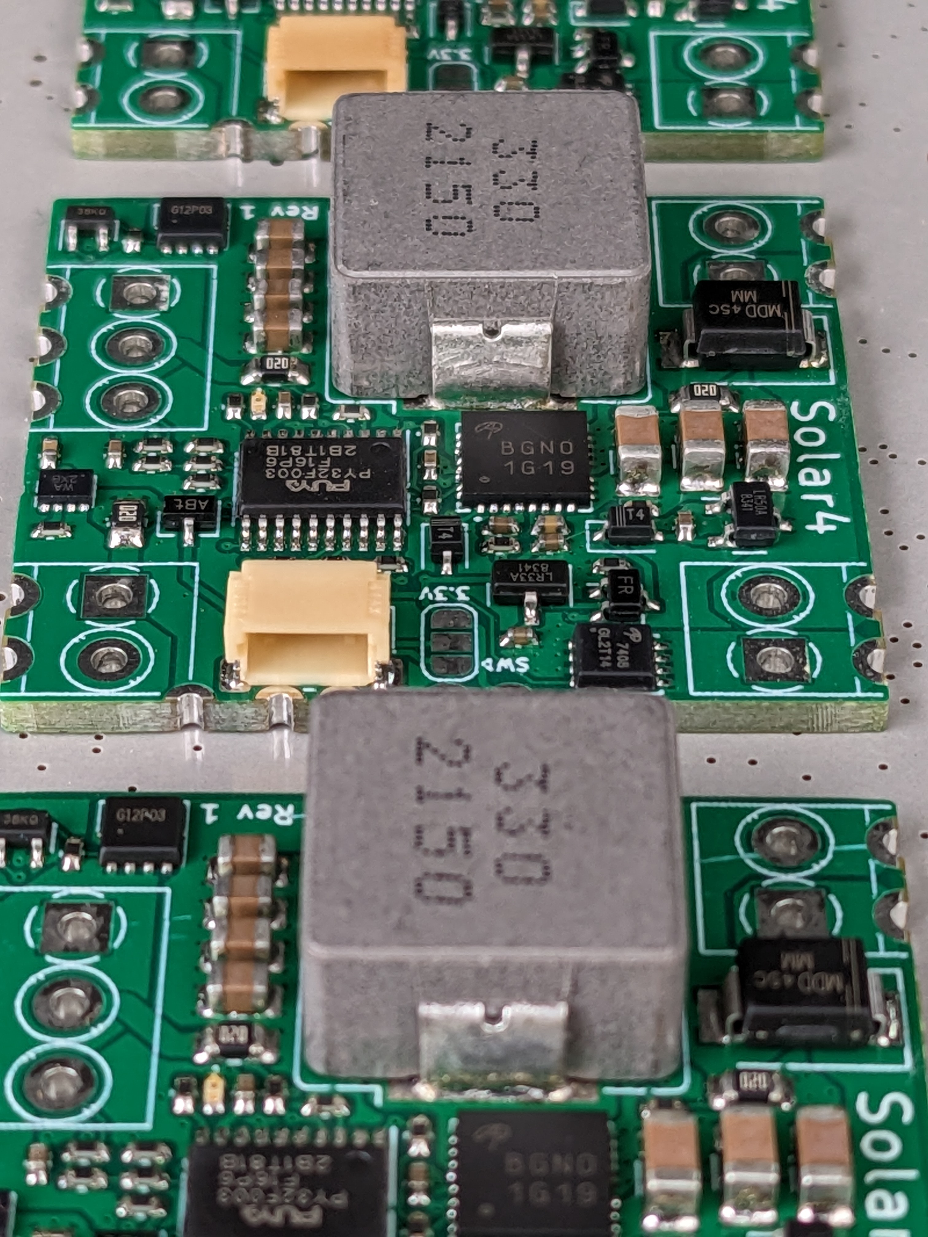
From left to right some major parts you can see are the AP22800 load switch on the far left, the PY32F003 microcontroller and the AOZ5316 DrMOS device. At the top left is a PMOS that disconnects the charger from the battery when inactive to prevent reverse leakage and at the bottom right an NMOS to drive the battery heater.
At the bottom you can see the Qwiic connector that can be used to configure the charger over I2C. The board can either be fitted with 3.5 mm screw terminals, have wires directly soldered to it, or be surface mounted to a carrier PCB using the castellated holes.
Initial power up test
Instead of immediately connecting a battery and checking whether any magic smoke escaped, I decided to be a little more careful. 🙂 I connected my bench power supply to the battery terminals and carefully ramped the voltage from 0 to 4.3 V. No high currents, no hot parts, no magic smoke. A good start!
Having achieved that confidence, I connected a LiFePO4 cell to the battery terminals and connected the bench power supply to the charge voltage input.
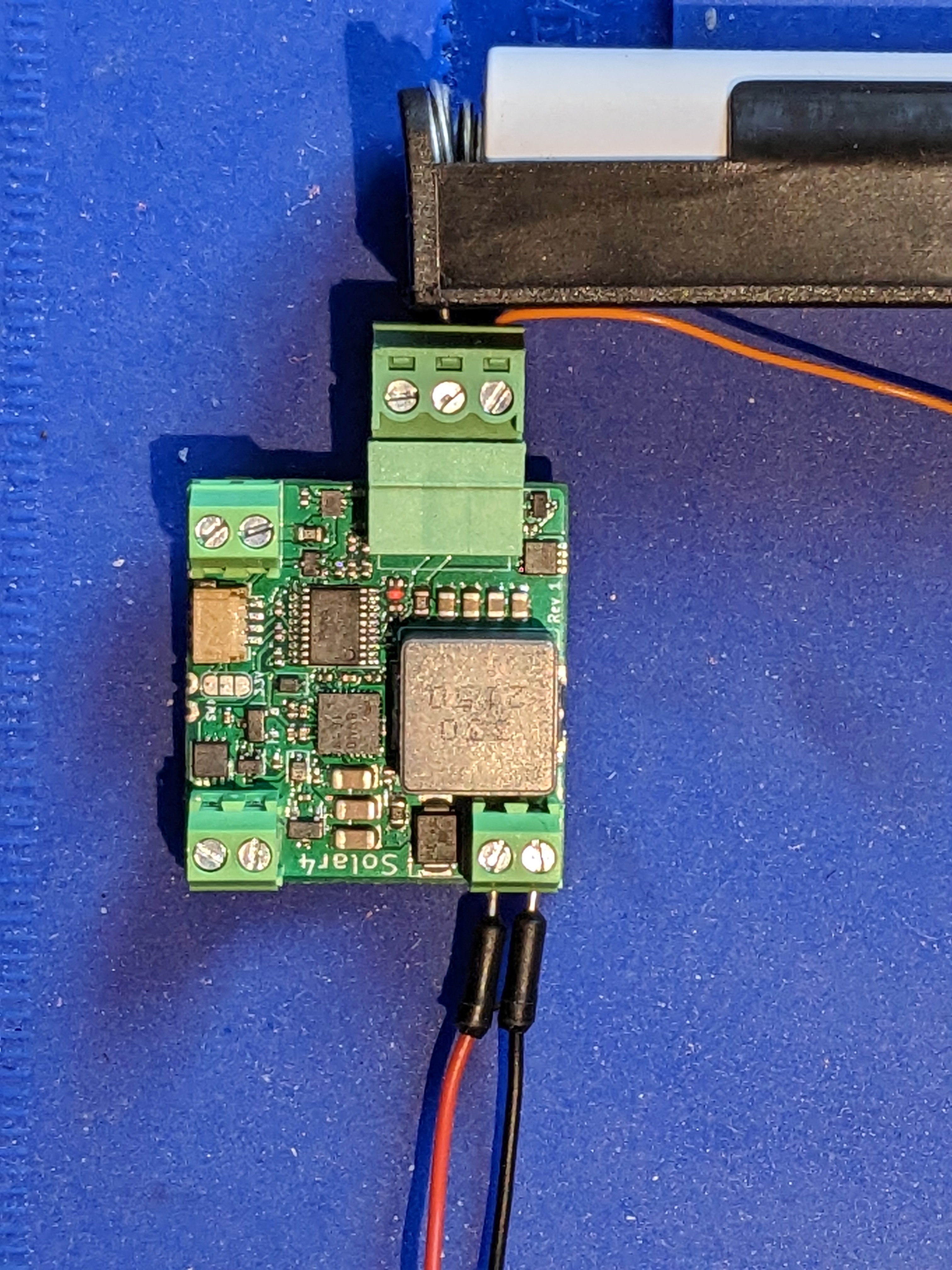
Ramping the input voltage up from 0 to 24 V again revealed no hot parts, excessive currents or magic smoke.
I also did a quick check of the system supply rail. One goal I want to achieve is to be able to support LTO cells and supercaps, and to do this I want to be able to run down to 1.8 V battery voltage. Another goal is to be able to run from input power in case the "battery" (more likely the supercap) is completely discharged. Normally you'd just combine the battery and input voltages through (Schottky) diodes, but the diode voltage drop would cause the minimum battery voltage at which the system can run to increase to 2.1 V or so. I designed a circuit to improve this situation and allow for both goals to be achieved, and a quick initial test seems to indicate it works as intended: the system supply can be powered from either battery or input voltage and the battery voltage drop is minimal. More testing is needed though to make sure no unintended current flows from the input to the battery.
Next steps
- More thorough testing of the supply cicruit
- Confirm lowest current draw of the complete circuit in sleep mode
- Write ADC measurement system code
- Write drivers for all peripherals
- Implement I2C access to be able to control all subsystems conveniently
- Test charging behavior using "manual" I2C control