PY32F003 PWM timer configuration
Pin assignment difficulties
One of the difficulties in most projects, and especially projects that try to accomplish a lot with very little, is doing the microcontroller pin assignments. For a serious mixed-mode project that tries to make the most of the available peripherals such as this one, this becomes especially tough.
I have to say that the PY32F003 actually does a pretty good job of making the peripherals available on many pins (see alternate pin assignment tables under 4.1, 4.2 and 4.3 in the datasheet at the time of writing). It's still a tough puzzle though.
My biggest issue was that all complementary-with-dead-time PWM timer outputs are mapped to pins that also have ADC input capability. It was especially frustrating that this also took one of the pins that have both ADC and analog comparator input capability out of the equation (PA3).
I was able to allocate pin PA1 to the battery current sense resistor so it should be able to serve both for battery current ADC measurement and overcurrent / short circuit protection using the comparator. I wanted to do the same thing for the load current, but ended up having to allocate two pins for this (ADC on PA7 and comparator on PB6).
Then there was the issue of how to turn the rectifier MOSFET off when the current reverses, to allow DCM mode. Or at least, be able to detect this before it can do damage by discharging battery current through the rectifier MOSFET.
After a lot of puzzling I came to the conclusion that the best way to deal with this would be to assign PB5 as timer 3 channel 2 input function to do an input capture when the external comparator detects that the current reverses, and use the ability for timers to be chained to somehow make this input capture on timer 3 do something to timer 1, in hardware. My hope was to be able to have the complementary (rectifier) PWM output go idle, thus allowing DCM.
If there's one thing I'd ask Puya to do in future chips, it is to make the complementary PWM outputs available on more alternate pins. That would have made my life a lot simpler.
Simple PWM for DrMOS
As explained in the overview post for this project, one charge topology I want to support is just a simple single PWM signal driving a DrMOS device. Since the DrMOS device has diode emulation mode built-in, driving it is trivial and just requires a single PWM output. The code to do so can be as simple as this:
/* Timer configuration */

void TimerConfig(void)
{
  /* Turn on the clock for the GPIOA block */
  LL_IOP_GRP1_EnableClock(LL_IOP_GRP1_PERIPH_GPIOA);

  /* Configure PA3 as TIM1_CH1 */
  LL_GPIO_SetPinMode(GPIOA, LL_GPIO_PIN_3, LL_GPIO_MODE_ALTERNATE);
  LL_GPIO_SetAFPin_0_7(GPIOA, LL_GPIO_PIN_3, LL_GPIO_AF_13);

  /* Single PWM output */
  LL_TIM_CC_EnableChannel(TIM1, LL_TIM_CHANNEL_CH1);
  LL_TIM_OC_ConfigOutput(TIM1, LL_TIM_CHANNEL_CH1,
                        LL_TIM_OCPOLARITY_HIGH | LL_TIM_OCIDLESTATE_LOW);
  LL_TIM_OC_SetMode(TIM1, LL_TIM_CHANNEL_CH1, LL_TIM_OCMODE_PWM1);
  LL_TIM_OC_SetPolarity(TIM1, LL_TIM_CHANNEL_CH1, LL_TIM_OCPOLARITY_HIGH);
  LL_TIM_OC_EnablePreload(TIM1, LL_TIM_CHANNEL_CH1);

  /* Some arbitrary timer compare value for testing */
  LL_TIM_OC_SetCompareCH1(TIM1, 150);

  /* Up count mode, as fast as we can (24 MHz) */
  LL_TIM_SetCounterMode(TIM1, LL_TIM_COUNTERMODE_UP);
  LL_TIM_SetClockDivision(TIM1, LL_TIM_CLOCKDIVISION_DIV1);
  LL_TIM_SetPrescaler(TIM1, 0);

  /* Test auto reload value, results in a PWM frequency of 16 kHz */
  LL_TIM_SetAutoReload(TIM1, 1500);

  /* Enable and start TIM1 PWM output */
  LL_TIM_GenerateEvent_UPDATE(TIM1);
  LL_TIM_EnableAllOutputs(TIM1);
  LL_TIM_EnableCounter(TIM1);
}
Complementary PWM with dead time and active rectifier
The other charge topology I want to support is an inverting buck-boost topology. Or, at least from the microcontroller's point of view, any topology where I have to manage the active rectifier MOSFET myself and prevent current from running out of the battery through the rectifier MOSFET if the systems ends up in DCM mode. The key to this is being able to detect when the current through the rectifier reverses (using an analog comparator) and doing something to stop it.
For DCM, the "something to stop it" would be to just turn the rectifier MOSFET off for the remainder of the PWM period. However, I could not find a way to do this, at least not with the timer chaining from TIM3 to TIM1 I ended up having to use to make my pin assignments work.
Instead, I found a way to do Critical Conduction Mode (CrCM) with the pin assignments available to me. This basically adjusts the PWM period by restarting the cycle (turn the rectifier MOSFET off and the switching MOSFET back on) when the inductor current reaches zero and starts to reverse.
The test code I used to test this scenario is below:
/* Timer configuration */

void TimerConfig(void)
{
  /* Turn on the clock for the GPIO used blocks */
  LL_IOP_GRP1_EnableClock(LL_IOP_GRP1_PERIPH_GPIOA |
                          LL_IOP_GRP1_PERIPH_GPIOB);

  /* Configure PA3 as TIM1_CH1 and PA0 as TIM1_CH1N */
  LL_GPIO_SetPinMode(GPIOA, LL_GPIO_PIN_3, LL_GPIO_MODE_ALTERNATE);
  LL_GPIO_SetPinMode(GPIOA, LL_GPIO_PIN_0, LL_GPIO_MODE_ALTERNATE);
  LL_GPIO_SetAFPin_0_7(GPIOA, LL_GPIO_PIN_3, LL_GPIO_AF_13);
  LL_GPIO_SetAFPin_0_7(GPIOA, LL_GPIO_PIN_0, LL_GPIO_AF_14);

  /* Configure PB5 as TIM3_CH2 to capture zero cross */
  LL_GPIO_SetPinMode(GPIOB, LL_GPIO_PIN_5, LL_GPIO_MODE_ALTERNATE);
  LL_GPIO_SetAFPin_0_7(GPIOB, LL_GPIO_PIN_5, LL_GPIO_AF_1);

  /* Turn on the TIM1 clock */
  LL_APB1_GRP2_EnableClock(LL_APB1_GRP2_PERIPH_TIM1);

  /* Complementary PWM outputs with dead time */
  LL_TIM_CC_EnableChannel(TIM1, LL_TIM_CHANNEL_CH1 | LL_TIM_CHANNEL_CH1N);
  LL_TIM_OC_ConfigOutput(TIM1, LL_TIM_CHANNEL_CH1,
                        LL_TIM_OCPOLARITY_HIGH | LL_TIM_OCIDLESTATE_LOW);
  LL_TIM_OC_SetMode(TIM1, LL_TIM_CHANNEL_CH1, LL_TIM_OCMODE_PWM1);
  LL_TIM_OC_SetPolarity(TIM1, LL_TIM_CHANNEL_CH1, LL_TIM_OCPOLARITY_HIGH);
  LL_TIM_OC_SetPolarity(TIM1, LL_TIM_CHANNEL_CH1N, LL_TIM_OCPOLARITY_HIGH);
  LL_TIM_OC_EnablePreload(TIM1, LL_TIM_CHANNEL_CH1);

  /* Some arbitrary dead time and timer compare value for testing */
  LL_TIM_OC_SetDeadTime(TIM1, 8);
  LL_TIM_OC_SetCompareCH1(TIM1, 150);

  /* Up count mode, as fast as we can (24 MHz) */
  LL_TIM_SetCounterMode(TIM1, LL_TIM_COUNTERMODE_UP);
  LL_TIM_SetClockDivision(TIM1, LL_TIM_CLOCKDIVISION_DIV1);
  LL_TIM_SetPrescaler(TIM1, 0);

  /* Test auto reload value, results in a PWM frequency of 16 kHz */
  LL_TIM_SetAutoReload(TIM1, 1500);

  /* Avoid Discontinuous Conduction Mode by running TIM1 in slave RESET mode,
   * triggered by TIM3 input capture */
  LL_TIM_SetSlaveMode(TIM1, LL_TIM_SLAVEMODE_RESET);
  LL_TIM_SetTriggerInput(TIM1, LL_TIM_TS_ITR2);

  /* TIM3 capture current zero cross */
  LL_APB1_GRP1_EnableClock(LL_APB1_GRP1_PERIPH_TIM3);
  LL_TIM_CC_EnableChannel(TIM3, LL_TIM_CHANNEL_CH1);
  LL_TIM_IC_Config(TIM3, LL_TIM_CHANNEL_CH1, LL_TIM_ACTIVEINPUT_INDIRECTTI |
                    LL_TIM_ICPSC_DIV1 | LL_TIM_IC_FILTER_FDIV1 |
                    LL_TIM_IC_POLARITY_FALLING);
  LL_TIM_SetCounterMode(TIM3, LL_TIM_COUNTERMODE_UP);
  LL_TIM_SetClockDivision(TIM3, LL_TIM_CLOCKDIVISION_DIV1);
  LL_TIM_SetPrescaler(TIM3, 0);
  LL_TIM_SetAutoReload(TIM3, 0xFFFF);

  /* Output signal to TIM1 on channel 1 input capture */
  LL_TIM_SetTriggerOutput(TIM3, LL_TIM_TRGO_CC1IF);
  LL_TIM_EnableCounter(TIM3);

  /* Enable TIM3 capture interrupt */
  LL_TIM_EnableIT_CC1(TIM3);
  NVIC_EnableIRQ(TIM3_IRQn);

  /* Enable and start TIM1 PWM output */
  LL_TIM_GenerateEvent_UPDATE(TIM1);
  LL_TIM_EnableAllOutputs(TIM1);
  LL_TIM_EnableCounter(TIM1);
}

/* TIM3 interrupt handler */

uint16_t last_cap;
uint16_t cap_period;

void TIM3_IRQHandler(void)
{
    uint16_t cap = LL_TIM_IC_GetCaptureCH1(TIM3);
    cap_period = cap - last_cap;
    last_cap = cap;
}
You may notice a couple of weird things in the code. For one thing, we are
using PB5 as TIM3 channel 2 in the pin assignment, but then set up TIM3
channel 1 in the code for input capture. This is because channel 1 seems
to be the only input capture channel that can send an output signal to TIM1.
Luckily, we can configure timer capture channel 1 to actually use TIM3_CH2
as input by specifying LL_TIM_ACTIVEINPUT_INDIRECTTI in the channel config.
Phew, almost foiled there! The devil is always in the details.
I used LL_TIM_IC_POLARITY_FALLING because that was the most convenient for
my test (see below). In an actual SMPS circuit the capture edge would depend
on the way the comparator is connected across the rectifying MOSFET.
One cool thing is that because we are using a timer input capture as the hardware connection to restart timer 1, we can get the actual PWM period that results for free by enabling the TIM3 interrupt and measuring the time between captures. We can use that in more advanced code, for instance to detect that we went from CCM to CrCM, and change the PWM parameters to keep the system in CCM; or if we're fine with running in CrCM mode, we can adjust the PWM on/off ratio based on the actually measured PWM period.
CrCM test
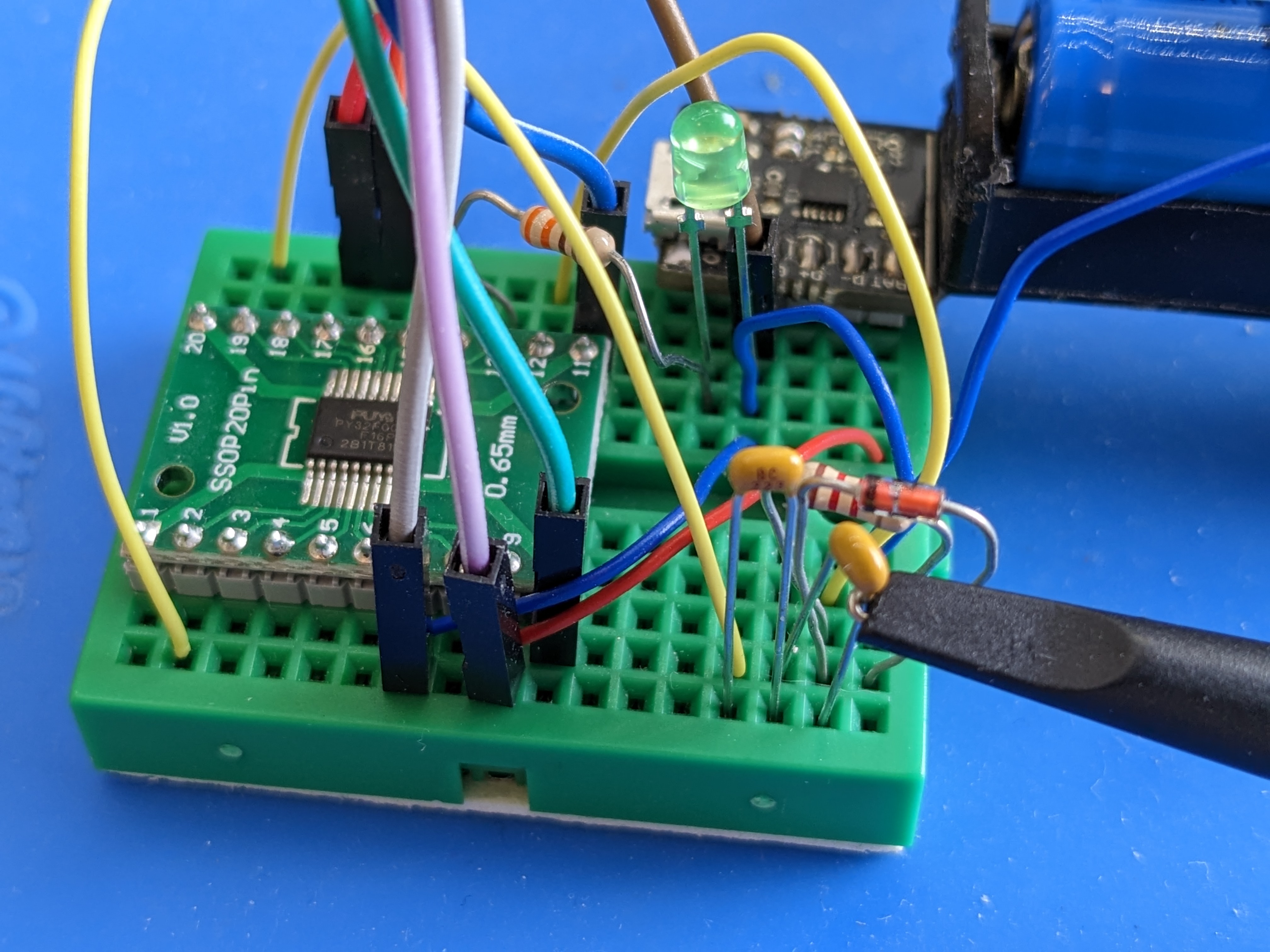
I was lazy and didn't want to actually hook up an SMPS stage or comparator, so the way I tested this was by running the active-high rectifier drive signal through a high-pass filter, and then just interpret the decaying analog signal with the digital input pin. Ugly, I know, but it served the purpose in this test.
Here's the test circuit:
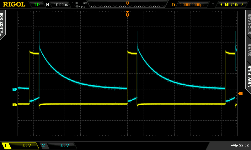
Scope channel 1 (yellow) measures the active-high switching MOSFET drive signal and channel 2 (blue) measures the high-pass filtered (differentiated) active-high complementary rectifier MOSFET drive signal. In the first scope capture, the fake comparator signal is not connected to detection pin PB5, hence, we get the programmed PWM frequency of about 16 kHz:
In the next scope capture, I connected the fake comparator signal to the detection pin PB5, which restarts the PWM period when it measures a "falling edge" (the analog signal reached the digital low threshold). No changes were made to the PWM parameters between the two captures, but as you can see below, the PWM period is significantly shorter now with a PWM frequency of around 69 kHz:
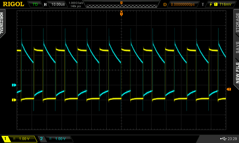
Adjusting the high-pass filter's RC time also allowed me to vary the PWM period in real time.